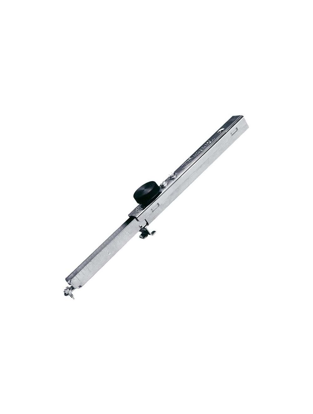
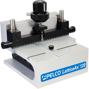
Electron Microscopy Sciences Lattice Scriber for Semiconductor Wafers
Shop Electron Microscopy Sciences Lattice Scriber for Semiconductor Wafers at

Fein Optic M46 Semiconductor Wafer Inspection Microscope
Electron Microscopy Sciences Lattice Scriber for Semiconductor Wafers
Wafers for Laboratories by Science Services

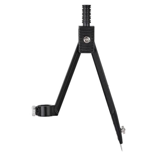
Electron Microscopy Sciences Wafer Cleaving Kit

PW topograph of a DH wafer after stripe diffusion-substrate

Sliding History-Dependent Adhesion of Nanoscale Silicon Contacts
Wafer Scribing / Wafer Cleaving - Mercia Semiconductor

Test structures are deployed in wafer scribe lines to measure and

Schematic illustration of corona charge-based, non-contact, in
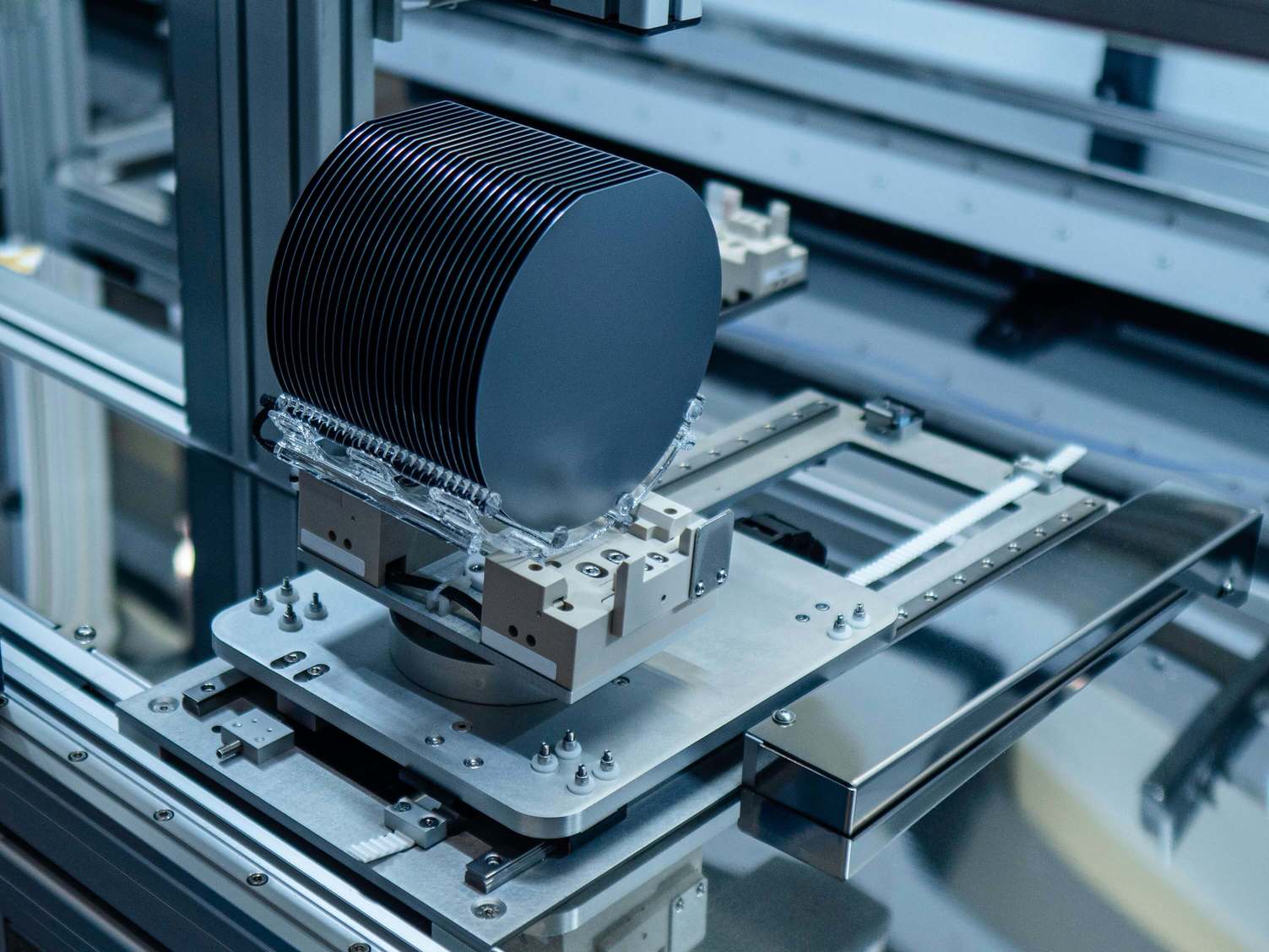
The Power of Silicon Wafers: Production, Properties and Application

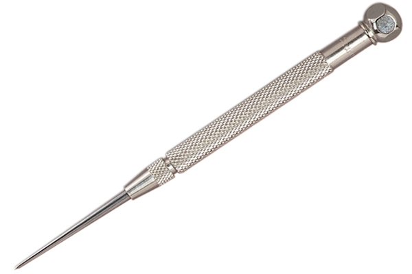
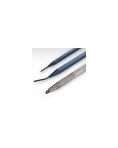
PELCO FlexScribe & FlipScribe Scribing Tool for Wafer Instruments
EMS Swiss Line Wafer Handling Tweezer Style 41LB8, Electron

Captivating Image of Si Silicon Crystal Lattice